
What Is PCB Design? Beginners Guide with Tips and Visuals
Understanding what is PCB design can help anyone involved in electronics, from hobbyists to professionals. This beginner-friendly guide from Arrival Electronics Limited explains the basics of printed circuit board creation and provides practical tips alongside visuals to clarify the process.
Mastering these principles not only improves product reliability but also enhances manufacturing efficiency. Whether designing simple circuits or complex multilayer boards, a solid foundation sets the stage for successful electronic projects.
What Is PCB Design?
Printed Circuit Board (PCB) design is the essential process of creating the layout and structure of a PCB, which provides mechanical support and electrical connections between components. Expert PCB design ensures that every board meets high standards for reliability and performance, whether used in consumer electronics or industrial applications.
PCBs form the foundation of virtually all modern electronic devices, making precise design a crucial step in successful product development. The design process involves carefully placing components and routing electrical pathways while considering manufacturability, signal integrity, and thermal management. This detailed approach helps produce quality products that consistently meet customer expectations and industry requirements.
The Core Steps in PCB Design
Design Definition and Schematic Capture
The PCB design process begins by defining the design concept and creating a detailed schematic diagram. This schematic represents all components and their electrical connections, serving as the foundational blueprint that guides the entire design and manufacturing process.Component Placement and Layout Implementation
Once the schematic is finalized, components are strategically placed on the board layout. This careful placement ensures optimal signal integrity, manufacturability, and thermal performance, which are essential for producing reliable and efficient electronic assemblies.Routing and Signal Integrity Optimization
The next step involves routing copper traces to electrically connect the components. This stage balances trace widths, spacing, and layer usage while minimizing electromagnetic interference and maintaining signal integrity particularly important for complex or high-frequency designs.Design for Manufacturability (DFM) and Validation
Automated and manual design rule checks verify compliance with manufacturing constraints and industry standards. This validation phase helps identify and resolve potential issues early, ensuring that the design is ready for smooth production and meets quality expectations.Generation of Manufacturing and Assembly Outputs
The final step is generating detailed manufacturing documentation, including Gerber files, drill data, Bill of Materials (BOM), and assembly drawings. These outputs provide precise instructions for fabrication and assembly, guaranteeing the physical PCB matches the intended design and performs as expected.
Key PCB Design Concepts and Terms
What PCB design services include:
Multi-layer PCB design, supporting boards with 20 or more layers for complex, compact circuit layouts.
Use of rigid and flex PCB technologies, including designs with blind and buried vias to optimize electrical connections between layers.
Expertise in controlled impedance and signal integrity analysis to ensure reliable performance in high-speed and sensitive electronic applications.
Delivery of detailed design documentation and technical data outputs, such as manufacturing drawings, assembly drawings, Bill of Materials (BOM), Gerber files, drill data, and 3D models to support smooth production and assembly.
These capabilities reflect a focus on advanced PCB design techniques and comprehensive documentation to meet demanding industry standards.
Tips for Effective PCB Design
Plan the Layout Early
Begin with a well-defined schematic and organize components logically. Grouping related components helps shorten signal paths and improves overall circuit performance.Follow Manufacturer Design Rules
Adhere strictly to the manufacturer’s specifications for trace widths, clearances, and hole sizes. Following these guidelines ensures the PCB is manufacturable and reduces the risk of production errors.Minimize Crosstalk and Noise
Route high-frequency signals with adequate spacing and consider shielding techniques. Incorporating ground planes helps reduce electromagnetic interference and improve signal integrity.Manage Thermal Performance
Place heat-generating components thoughtfully to avoid hotspots. Use thermal vias or heat sinks when necessary to maintain safe operating temperatures and ensure reliability.Use Layer Stacking Effectively
Multilayer PCBs provide better routing options and improved signal integrity, especially for complex designs. However, they also increase manufacturing complexity and cost, so careful planning is essential.Review, Simulate, and Iterate
Conduct design rule checks (DRC) and run simulations to identify and correct errors early in the process. Iterating the design based on these insights leads to enhanced performance and manufacturability.
These tips reflect widely accepted what is PCB design best practices consistent with the professional and thorough approach expected in high-quality PCB design services.
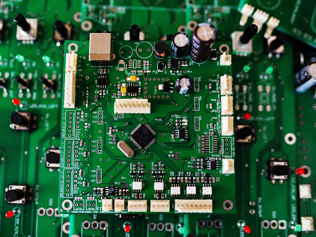
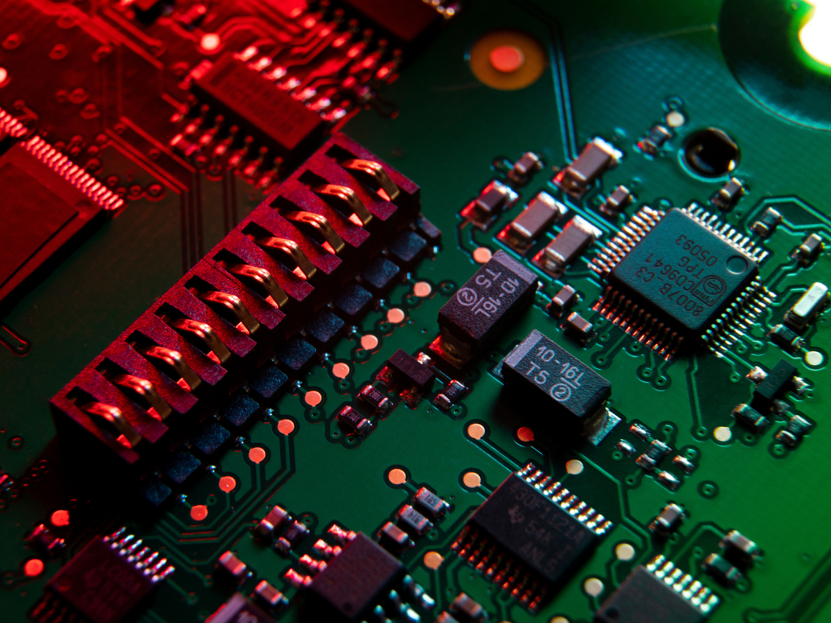
Visual Overview of PCB Design Process
Schematic Capture Example
This initial stage involves creating a circuit diagram that visually represents electronic components such as resistors, capacitors, and integrated circuits (ICs) connected by lines indicating electrical connections. The schematic serves as the foundational blueprint for the PCB layout.Component Placement Diagram
After the schematic is complete, components are arranged logically on the PCB outline. Proper grouping and orientation of components optimize signal flow, manufacturability, and thermal management.Routing Example
Copper traces are drawn to electrically connect component pads. This routing maintains clear spacing and uses vias to transition connections between layers, ensuring signal integrity and manufacturability.Design Rule Check (DRC) Highlight
Automated design rule checks flag any violations, such as insufficient spacing or incorrect trace widths. These checks help prevent errors that could affect production and functionality.Manufacturing File Output
The final design stage generates manufacturing files, including Gerber files that define copper layers, solder masks, and drill data. These files provide precise instructions required for accurate fabrication and assembly of the PCB.
This overview reflects a professional and thorough PCB design process supported by industry best practices and aligned with the capabilities expected from expert PCB design services.
Why PCB Design Matters in Electronics Manufacturing
A well-executed PCB design is crucial for minimizing manufacturing errors and reducing production costs. Careful design ensures that components are accurately placed and electrically connected, which directly improves device reliability and performance.
Effective PCB design also helps products comply with industry standards related to safety, durability, and electromagnetic compatibility (EMC). This compliance is essential for market approval and long-term product success.
For manufacturers, the PCB design serves as the detailed blueprint that guides fabrication and assembly processes. It ensures that all components fit together precisely and function as intended, supporting consistent quality and efficient production.
Common Questions About PCB Design
What is the difference between PCB design and PCB layout?
PCB design includes the entire process of creating the schematic and board layout, while PCB layout refers specifically to arranging components and routing traces on the board.How long does it take to design a PCB?
The time varies depending on complexity, from a few hours for simple boards to several weeks for multilayer, high-speed designs.What software is best for beginners?
KiCad and Eagle are user-friendly options for beginners, offering sufficient features for most entry-level projects.Can PCB design affect product reliability?
Yes, poor design can lead to signal issues, overheating, or manufacturing defects that compromise product function.What is a Gerber file?
Gerber files are the standard output files used by PCB manufacturers to fabricate the physical board layers.
Turning Insights Into Action
Understanding what is PCB design is crucial for anyone involved in electronic product development. From initial schematics to final manufacturing files, the design process requires careful planning and attention to detail. Using recommended practices and modern tools can ensure the production of reliable, efficient printed circuit boards.
For companies seeking professional assistance or advanced PCB design solutions, Arrival Electronics Limited offers expert guidance tailored to project needs.
Visit arrivalelectronics.co.uk for further information.