
How PCB Production and Assembly Works Step by Step Guide
PCB production and assembly is the backbone of modern electronics. Arrival Electronics Limited ensures that every project meets the highest standards of quality and reliability. This step-by-step guide covers each stage of PCB manufacturing and assembly, from design and material selection to component placement and testing.
Following a structured workflow not only improves efficiency but also reduces errors, delivering high-quality results for every project. By understanding each step of the process, businesses can make informed decisions and achieve consistent, dependable PCB performance.
Understanding the Process
The process encompasses creating printed circuit boards from initial design to a fully functional product. This includes fabrication, component placement, soldering, and thorough testing to ensure reliability and performance.
Each stage requires careful attention to detail and adherence to industry standards to prevent defects. By following a structured workflow, manufacturers can achieve consistent quality and optimal functionality for all electronic devices. Proper documentation and quality checks at every step further enhance the overall reliability of the finished boards. Implementing these best practices also helps reduce production delays and lowers the risk of costly rework.
What is PCB Production?
PCB production and assembly begins with the fabrication of the bare board. This includes:
Design translation: Converting circuit designs into manufacturing files (Gerber files). This ensures the design is accurately represented for production.
Substrate selection: Choosing materials like FR4, PTFE, or ceramic. The material affects durability, heat resistance, and signal integrity.
Layer creation: Laminating multiple layers for complex boards. Proper lamination prevents misalignment and ensures structural stability.
Etching and drilling: Creating the copper traces and vias. Precision in this step is critical for electrical performance and connectivity.
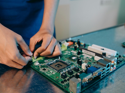
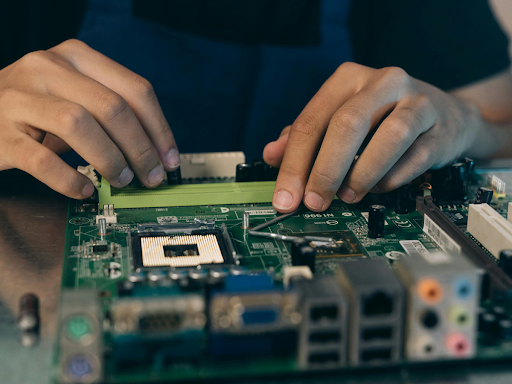
How PCB Assembly Works
PCB assembly involves mounting electronic components onto the fabricated board, making it functional. Key steps include:
Solder paste application: Applying solder paste to the board pads. This step ensures components will properly adhere during soldering.
Component placement: Using pick-and-place machines or manual assembly. Accurate placement is critical for circuit performance and reliability.
Reflow soldering: Melting the solder to secure components. Proper temperature control prevents damage to sensitive components.
Inspection: Automated Optical Inspection (AOI) or manual checks. Thorough inspection catches defects early, reducing rework.
Testing: Functional tests ensure reliability. These tests verify that the assembled board meets design specifications and operates correctly.
Complete PCB Assembly Workflow
Step 1: Design Review and DFM
Before production, Arrival Electronics conducts a Design for Manufacturability (DFM) review. This ensures:
Optimal component placement
Correct trace widths and spacing
Manufacturable board layers
Step 2: Material Selection
Selecting the right materials affects durability and signal integrity. Common substrates include:
FR4: Standard for most boards
Polyimide: Flexible applications
Ceramic: High-frequency or heat-resistant boards
Step 3: PCB Fabrication
Layer lamination: Multiple layers pressed together
Etching: Removing excess copper to form circuit patterns
Drilling: Making holes for through-hole components and vias
Surface finishing: Protecting exposed copper
Step 4: Solder Paste Application
Solder paste is applied to pads where components will be mounted. Precision is key for surface-mount devices (SMD).
Step 5: Component Placement
SMT components: Placed using automated pick-and-place machines
Through-hole components: Inserted manually or by machine
Step 6: Reflow Soldering
The board passes through a reflow oven, melting the solder and securing components in place. Careful temperature control during this stage ensures components are not damaged and solder joints remain strong and reliable.
Step 7: Inspection and Quality Control
Quality checks include:
Automated Optical Inspection (AOI)
X-ray inspection for hidden solder joints
Functional testing to verify performance
Step 8: Final Assembly and Packaging
Boards are cleaned, conformal coated if needed, and packaged for delivery. Proper finishing and packaging protect the boards during transport and ensure they arrive in optimal condition for installation.
Emerging PCB Trends for 2025
High-Density Interconnect (HDI) PCBs: Boards with finer lines and smaller vias for compact, high-performance devices.
Flexible and Rigid-Flex Designs: PCBs that bend or combine rigid and flexible sections for innovative applications.
Advanced Thermal Management Materials: Materials designed to dissipate heat efficiently in high-power electronics.
Sustainable Manufacturing Practices: Eco-friendly processes and materials to reduce environmental impact.
AI-Assisted Assembly and Inspection: Using artificial intelligence to improve placement accuracy and detect defects faster.
Benefits of a Detailed PCB Assembly Process
Ensures high reliability: Following a structured process minimizes defects and ensures consistent board performance.
Reduces assembly errors: Careful step-by-step procedures help prevent misaligned components or soldering issues.
Improves production efficiency: Streamlined workflows save time and resources, allowing faster project completion.
Guarantees compliance with industry standards: Adhering to standards ensures boards meet regulatory and quality requirements.
Enhances overall product quality: Thorough processes and inspections lead to durable, high-performing final boards.
Your Questions Answered
What is the difference between production and assembly?
Production involves fabricating the bare board, while assembly adds electronic components to make it functional.How long does the process take?
Standard production can take 1–3 weeks depending on complexity; prototyping may take less.What are common assembly errors?
Errors include misaligned components, solder bridges, and cold joints. Inspection processes catch these issues.Can I choose materials for my boards?
Yes, materials like FR4, polyimide, and ceramic can be selected based on performance needsWhat testing methods are used after assembly?
Automated Optical Inspection (AOI), X-ray, in-circuit testing, and functional tests are common.Are flexible boards included in production?
Yes, flexible and rigid-flex designs are available for various applications.
Ensuring Quality in Every PCB Project
Following a structured production and assembly process ensures reliability, efficiency, and high-quality boards. By carefully managing each step from design and material selection to component placement and testing manufacturers can reduce errors and improve overall performance.
Arrival Electronics Limited provides expert guidance and support throughout the PCB production and assembly process, helping clients achieve consistent, dependable results. Working with experienced professionals also ensures that projects stay on schedule and meet industry standards. Adopting a methodical approach ultimately leads to stronger, more reliable electronics that perform consistently in real-world applications.