
A Practical PCB Design Guide for Beginners and Pros
Printed Circuit Boards (PCBs) are the backbone of modern electronics, found in devices from smartphones to medical equipment. Understanding electronic components and how they interact is essential for anyone involved in pcb design, and Arrival Electronics Limited provides practical guidance and professional insights for engineers, designers, and hobbyists.
Understanding PCBs and Electronic Components
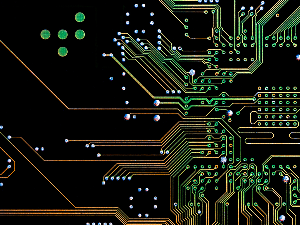
A PCB is a flat board that physically supports and electrically connects electronic components through conductive pathways. Components such as resistors, capacitors, diodes, transistors, and integrated circuits (ICs) are soldered onto PCBs to create fully functioning circuits.
Key Electronic Components in Circuit Boards:
Resistors: Control current flow and adjust signal levels.
Capacitors: Store and release electrical energy, smoothing voltage fluctuations.
Diodes: Ensure current flows in one direction, protecting sensitive components.
Transistors: Function as switches or amplifiers, regulating current and signal flow.
Integrated Circuits (ICs): Combine multiple components in a compact package to perform complex operations.
Each component’s role must be understood before starting the board layout to avoid errors during manufacturing or testing
Step 1: Defining Your Project Requirements
Every successful PCB begins with clear project specifications:
Functionality: Determine what the PCB should achieve. Will it power a device, manage signals, or control systems?
Size Constraints: Consider the physical dimensions of the device and component sizes.
Power Requirements: Account for voltage, current, and thermal considerations.
Environmental Conditions: Components should be selected based on operating temperatures, humidity, or exposure to vibration and chemicals.
For instance, a PCB for an outdoor IoT sensor might require waterproof components, while a wearable device will need low-profile SMD components.
Step 2: Schematic Design
Creating a schematic is a critical first step in developing a circuit board. Schematic diagrams visually represent the connections between components and help engineers validate circuit functionality before building a physical board.
Tools commonly used include:
KiCad: Free and open-source software suitable for beginners and professionals.
Eagle: Offers user-friendly features for small to medium projects.
Altium Designer: Advanced tool for complex, professional-grade electronic layouts.
A well-organized schematic reduces errors during PCB layout and improves manufacturability.
Step 3: Component Selection and Sourcing
Choosing the right electronic components is crucial for successful PCB performance. Factors to consider include:
Availability: Select components that are in stock or have reliable lead times.
Cost: Balance quality, performance, and budget.
Footprint: Ensure components fit the intended PCB layout.
Lifecycle Considerations: Avoid components nearing obsolescence to prevent supply issues.
Smart Sourcing Tips:
Use Component Kitting to group all required parts for a PCB assembly, ensuring availability and consistency.
Maintain a list of alternatives for critical components to prevent redesign delays during shortages.
Work with trusted distributors to reduce the risk of counterfeit parts, which can compromise product safety.
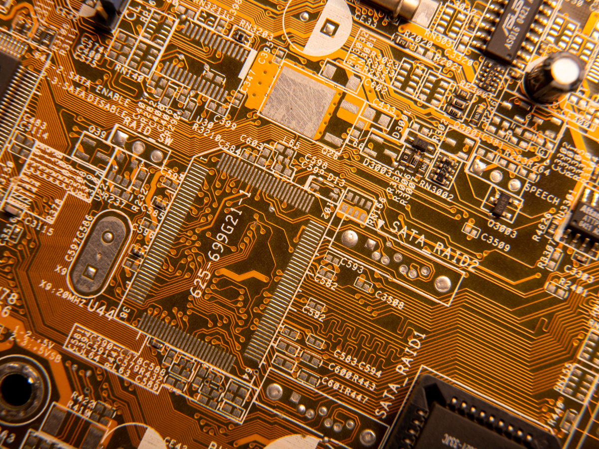
Step 4: PCB Layout Design
After finalizing the schematic and components, the next step is physical PCB layout.
Best Practices for Layout:
Component Placement: Place components logically to minimize trace lengths. Keep high-speed or sensitive components close to related ICs to reduce signal noise.
Routing: Connect components with traces, avoiding sharp angles to reduce EMI (electromagnetic interference). Use appropriate trace widths for current-carrying capacity.
Ground Planes and Power Distribution: Include solid ground planes for stability. Use power planes to ensure even voltage distribution across the board.
Thermal Management: Ensure heat-generating components have proper spacing. Consider thermal vias or heat sinks for high-power circuits.
Example: PCB for a 5V Power Supply
Components: Voltage regulator IC, capacitors, resistors, and diodes.
Layout: Input voltage flows through the regulator; capacitors filter voltage spikes; resistors set output levels.
Practical Tip: Keep the regulator and heat-generating components spaced to allow airflow, preventing overheating.
Step 5: Design Verification and Testing
Before sending a PCB for manufacturing:
Design Rule Check (DRC): Identifies trace width violations, spacing issues, or component overlaps.
Electrical Rule Check (ERC): Verifies electrical connectivity.
Simulation: Some advanced tools allow testing signal integrity and thermal performance virtually.
These steps prevent manufacturing errors and reduce costly revisions.
Step 6: Manufacturing Considerations
PCBs are fabricated using Gerber files, which contain all necessary information for production. Manufacturers rely on these files for:
Copper layers: Defines electrical pathways.
Drill data: Placement of vias and holes.
Solder masks: ProtectGet expert guidance tailored to your project needs. areas of the board during assembly.
Common Challenges and Practical Solutions in Circuit Development
Signal Integrity: Use ground planes, proper trace routing, and differential pairs for high-speed signals.
Thermal Management: Add heat sinks, thermal vias, and ensure proper component spacing.
Component Availability: Maintain a list of alternative components and use component kitting to streamline assembly.
Counterfeit Parts: Source from authorized distributors and inspect incoming components.
FAQ
1. What are the most common electronic components used in PCBs?
Resistors, capacitors, diodes, transistors, and integrated circuits (ICs) are the most commonly used components.
2. How can I prevent counterfeit parts in my PCB assembly?
Source components from authorized distributors, inspect incoming parts, and maintain a list of approved vendors.
3. What is component kitting?
Component kitting is the process of collecting and organizing all required parts for PCB assembly, ensuring availability and reducing assembly errors.
4. Why is PCB layout important?
Proper layout reduces noise, improves thermal management, and ensures reliable signal integrity.
5. How do I select the right components for my design?
Consider availability, cost, size, lifecycle, and electrical specifications to choose components that match your project requirements.
6. What is a Gerber file?
A Gerber file is the standard format used to convey circuit board data to manufacturers for production.
Conclusion
Successful PCB design requires a combination of technical expertise, practical experience, and meticulous planning. By understanding electronic components, implementing smart sourcing, planning for obsolescence, and preventing counterfeit parts, engineers can create reliable, high-quality boards.
For professional PCB assembly, component sourcing, and electronic manufacturing services, visit Arrival Electronics Limited. Their expertise in component kitting and PCB production ensures your designs move from concept to reality efficiently.
Turn Ideas into Action with a Personalized Design Consultation
Request Design Consultation: Get expert guidance tailored to your project needs.
Contact Now : Reach out today to start your design journey.